
The Layer Stack and Thermal Bottleneck Breakthroughs in the HBM3E-to-HBM4 Upgrade
Upgrading from HBM3E to HBM4 represents one of the most technically challenging—and most consequential—evolutions in modern memory engineering. HBM4 promises higher signaling rates, greater per-die capacity, and improved energy efficiency per bit, but achieving those gains requires rethinking the layer stack, interconnect strategies, and thermal management at the package level.

What changes between HBM3E and HBM4
At a high level, HBM4 aims to increase per-channel bandwidth, raise per-die capacity, and reduce power per bit compared with HBM3E. Practically, this manifests as:
- Higher data rates per pin, moving signaling into substantially faster regimes requiring improved SI (signal integrity) and jitter control.
- Larger die capacities and potentially more die per stack, which increases thermal density and mechanical complexity.
- More aggressive power-performance trade-offs, including finer-grained voltage islands and more complex power-delivery networks inside packages.
These changes mean that the physical layer stack—die geometry, TSV and micro-bump layouts, interposer routing, and package substrate—must evolve. Simultaneously, thermal solutions must scale to dissipate more power per unit area while preserving the electrical performance needed for high-speed signaling.
Layer stack innovations enabling HBM4
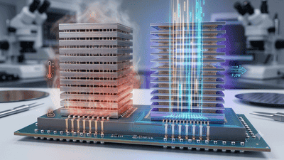
The layer stack in HBM4 reflects multiple concurrent adjustments across die, interposer, and substrate layers. Key innovations include:
- Heterogeneous die-thickness design: Rather than uniform die thickness across all DRAM layers, HBM4 stacks use varied die thickness optimized for TSV density, thermal pathing, and mechanical stress reduction. Thinner top dies reduce TSV seam stress and improve hybrid-bonding alignment, while thicker bottom dies maintain mechanical strength.
- High-density hybrid bonding planes: HBM4 increases the number and density of hybrid-bond pads between dies and between die and interposer. These bonding planes use copper-based direct bonds with finer pitch than HBM3E, enabling higher per-channel signaling while reducing parasitic capacitance relative to micro-bumps.
- Distributed TSV / micro-via topologies: TSV placement patterns evolve to minimize crosstalk and reduce via-induced thermal hotspots. HBM4 leverages staggered TSV arrangements and smaller-diameter TSVs in conjunction with redistribution layers (RDLs) to maintain routing density without sacrificing mechanical reliability.
- Active interposer regions: Whereas earlier interposers were largely passive silicon routing fabrics, HBM4 interposers increasingly include active elements—power-distribution meshes, embedded decoupling capacitors, and localized signal conditioning (equalizers) fabricated using foundry logic processes on sections of the interposer. This offloads some SI and PDN complexity from the compute die and the memory stacks, improving overall package performance.
- Advanced RDL materials and fine-pitch trace stacks: New RDL dielectrics and copper trace metallurgy allow finer traces with lower loss at high frequencies, improving channel performance across the interposer and package substrate.
Together, these layer-stack innovations reduce parasitics, improve impedance control, and provide more reliable high-speed paths for HBM4 signaling. However, structural and electrical gains alone are insufficient without addressing the thermal consequences of denser stacks and higher signaling rates.
Thermal bottlenecks introduced by HBM4
HBM4’s higher per-die capacity and increased signaling rates both elevate power density. Thermal bottlenecks present in HBM3E are amplified by HBM4 in several ways:
- Increased local heat flux: More active DRAM and faster signaling raise heat generation per mm², especially near TSV clusters and high-activity regions of the memory stack.
- Thermal coupling with compute die: Co-packaged accelerators generate significant heat themselves, and the proximity of compute die and HBM stacks intensifies thermal coupling, requiring package-level thermal co-design.
- Reduced thermal path length: As die get thinner for electrical reasons, the available conduction path for heat to escape through die bulk is reduced, making interface thermal resistance more significant.
- Hotspot-driven reliability limits: Elevated temperatures accelerate electromigration, degradation of bonding interfaces, and retention/power cycling stress on DRAM cells, reducing long-term reliability unless mitigated.
Addressing these bottlenecks demanded breakthroughs in materials, mechanical design, and cooling strategies.
Breakthrough 1 — Embedded microfluidic cooling channels

One of the most transformative advances enabling HBM4 adoption is the integration of embedded microfluidic cooling channels into the package substrate and, in some experimental designs, within the interposer. Key aspects:
- Microchannel placement: Channels are routed beneath high-heat-density areas—directly under the compute die and aligned with the hottest regions of HBM stacks—providing localized convective cooling.
- Materials and reliability: Channel walls and seals use polymer or silicon-glass composites engineered for thermal expansion compatibility and chemical resistance to common dielectric coolants (e.g., engineered fluoroinert fluids).
Microfluidic cooling reduces local thermal resistance and flattens temperature gradients across the stack, enabling higher sustained frequencies and supporting larger die counts per stack without breaching reliability thresholds.
Breakthrough 2 — Thermally conductive but electrically insulating interlayer films
Traditional die attach and underfill materials present a trade-off: many thermally conductive materials are electrically conductive and therefore unsuitable near fine-pitch interconnects. New interlayer films used in HBM4 are engineered to be both highly thermally conductive and electrically insulating, enabling tighter thermal coupling between dies and the interposer without risking shorts or leakage.
- High thermal conductivity polymers: Filled polymer films with aligned boron nitride, graphene, or metal-oxide flakes reach thermal conductivities far above legacy underfills while maintaining dielectric strength.
- Thin-film integration: These films are applied in micro-thicknesses that keep bondline resistance low and permit high-precision hybrid bonding without introducing mechanical separation.
- Improved TIM performance: Replacing bulky TIMs with these thin films reduces interface thermal resistance and supports thinner overall packages with better mechanical stability.
By improving heat conduction across bonding interfaces, these films help HBM4 stacks move heat into interposer-inserted thermal vias or directly into microfluidic channels.
Breakthrough 3 — Active thermal management with embedded sensors and local throttling

HBM4 packages increasingly incorporate thousands of embedded temperature sensors distributed through the interposer and die stacks. These sensors feed a local thermal management controller that performs ultra-fast, localized throttling and power redistribution to prevent hotspots from exceeding safe thresholds.
- Granular control: Instead of single-package throttling, HBM4 allows per-die or per-region frequency and voltage modulation, smoothing thermal transients and preserving average performance.
- Predictive algorithms: Machine-learning-based thermal predictors anticipate workload-driven hotspots and preemptively adjust DVFS (dynamic voltage and frequency scaling) at fine granularity.
- Closed-loop liquid control: In microfluidic designs, sensor data can dynamically adjust coolant flow rates and temperature setpoints to prioritize critical hotspots.
This active approach preserves performance under bursty AI workloads, reduces thermal cycling stress, and extends device lifetime compared with coarse binary thermal throttling.
Breakthrough 4 — TSV and micro-via thermal engineering
Thermal pathways through TSVs and micro-vias are both a blessing and a challenge. New TSV designs in HBM4 optimize for both electrical isolation and thermal conduction:
- Thermally enhanced TSVs: Introducing dedicated thermal TSVs—metal-filled vias not used for signaling—creates low-resistance thermal paths from inner dies to interposer thermal sinks.
- Composite via metallurgy: TSVs use composite liners combining copper for conduction and thin high-k dielectrics to maintain electrical isolation where needed.
- Staggered via planning: Placing thermal TSVs in staggered arrays avoids creating electrical crosstalk patterns while maximizing thermal extraction across the stack footprint.
These TSV-centric strategies significantly reduce vertical thermal resistance and let package-level cooling remove heat more uniformly as stacks grow taller or denser.
Breakthrough 5 — Co-design of power-delivery networks (PDN) and thermal paths
Electro-thermal co-design has become a core part of HBM4 engineering. PDNs are designed so that high-current delivery paths double as thermal conduits, and package-level capacitors are placed to balance electrical decoupling with thermal distribution.
- PDN segmentation: Creating distributed PDN islands reduces local IR drop and keeps high-current loops short, lowering localized Joule heating.
- Thermally-aware decoupling: Bulk decoupling capacitors are placed not only for SI but also to spread heat and reduce hotspots caused by rapid current transients.
- Integrated heatspreaders: PDN planes are tied to embedded heatspreaders and thermal vias to move heat laterally to coolant-bearing regions.
Co-designed PDNs improve both performance stability and lifetime by ensuring that power and heat flow synergize rather than conflict within tightly stacked packages.
Materials and manufacturing innovations that enable scale
Beyond architecture, manufacturing advances have been crucial to bringing HBM4 into volume production:
- Improved hybrid-bond tooling: High-throughput, sub-micron alignment tools reduce bond defects at fine pitch, increasing yield for high-density bonding planes.
- Advanced underfills and low-stress adhesives: Materials that reduce mechanical warpage during thermal cycling improve reliability for taller stacks.
- High-precision die thinning: Consistent ultra-thin die production reduces mechanical strain and ensures uniform thermal conduction across stacks.
- Automated test coverage: New wafer- and package-level test flows with built-in thermal stress testing accelerate qualification while measuring real-world thermal behavior.
Combining these manufacturing improvements with the architectural breakthroughs above enables suppliers to scale HBM4 production while preserving acceptable yields and reliability metrics.
System-level impacts and use cases
With thermal and layer-stack bottlenecks addressed, HBM4 unlocks new system capabilities across several domains:
- AI training: Higher sustained memory bandwidth and larger on-package capacity reduce inter-node communication and allow larger model partitions per accelerator.
- Inference at scale: Efficient HBM4 packages support high-throughput inference engines with better performance-per-watt in dense rack configurations.
- HPC and scientific computing: Simulation workloads that require massive memory bandwidth and low latency benefit from HBM4’s improved throughput.
- Edge HPC: Microfluidic cooling and compact CoWoS-style packages allow higher-performance edge devices where ambient cooling is limited but high compute is required.
For system designers, HBM4 means more design freedom but also new integration responsibilities—thermal plumbing, coolant routing, and power distribution become part of system bills of materials and design cycles rather than afterthoughts.
Reliability, testing, and qualification
As with any major packaging advance, ensuring long-term reliability is essential. HBM4 qualification regimes focus on:
- Accelerated thermal cycling and thermal shock tests reflecting microfluidic and cold-plate environments.
- Extended electromigration testing under high-frequency switching to validate bond integrity and interconnect lifetime.
- Retention and data-integrity stress across elevated temperature and voltage corner cases for larger die and stacked configurations.
- System-level soak testing to account for thermal interaction between compute die and HBM stacks under representative workloads.
Data from early production lines indicate that packages adopting the combined microfluidic + thermally conductive film + active sensor approach meet or exceed the reliability targets set for HBM3E, even under more aggressive performance envelopes—provided manufacturing controls are strict and test coverage is comprehensive.
Economic and supply-chain consequences
The technical breakthroughs enabling HBM4 carry supply-chain and economic implications:
- Higher ASPs for HBM4 modules: Premium packaging and integrated cooling will command higher average selling prices compared with HBM3E, at least initially.
- OSAT specialization premium: Vendors capable of reliable microfluidic integration and fine-pitch hybrid bonding will command premiums for their services.
- Increased capital intensity: Scaling microfluidic-enabled packaging lines and active-interposer fabrication requires new capital and specialized workforce skills.
- Customer procurement shifts: Hyperscalers and OEMs will likely favor suppliers offering validated HBM4 packages with integrated thermal solutions, locking in demand through long-term agreements and co-investments.
Overall, the first wave of HBM4 production will likely be allocated to large, strategic customers with tight co-design relationships; broad adoption will follow as costs fall and supply ramps.
What to watch in the next 12–24 months
Key signals will determine how rapidly HBM4 becomes mainstream:
- Published field data from early hyperscaler deployments showing real-world performance and cooling trade-offs.
- Announcements of OSAT and IDM capacity expansions for hybrid bonding, microfluidic integration, and active-interposer fabrication.
- Standardization efforts around microfluidic interfaces, coolant types, and package mechanical mounts to ensure interoperability across vendors and systems.
- Tooling advances that reduce hybrid-bond defect rates and increase throughput, lowering per-unit packaging costs.
As these signals accumulate, expect the premium for HBM4 to compress and for designers to move it from bleeding-edge to production-grade for top-tier accelerator and HPC products.
Practical recommendations for engineers and procurement teams
If you are designing systems that will use HBM4 in the near term, consider the following actions:
- Start early with thermal co-design: Engage packaging and cooling teams during architecture definition, not at final integration.
- Qualify multiple suppliers: Packaging yields and interconnect choices vary; diversify early to reduce supply risk.
- Plan for coolant infrastructure: Rack-level coolant plumbing, coolant monitoring, and leak mitigation must be part of procurement and data-center ops planning.
- Budget for higher initial costs: Early HBM4 modules will carry premiums; evaluate system-level benefits in density and power savings across TCO, not unit price alone.
- Insist on rigorous test reports: Request detailed electro-thermal and reliability data from suppliers, including thermal cycling, electromigration, and retention tests under expected workloads.
Conclusion
The move from HBM3E to HBM4 is more than an incremental speed bump; it is an architectural and manufacturing inflection point that ties together layer-stack innovation with package-level thermal breakthroughs. Embedded microfluidics, thermally conductive insulating films, active sensing and control, TSV thermal engineering, and PDN-thermal co-design collectively remove the thermal and mechanical barriers that once constrained higher stack counts and faster signaling. These innovations enable HBM4 to deliver the bandwidth, capacity, and energy efficiency next-generation AI, HPC, and accelerator systems demand.
Adoption will follow a classic technology diffusion curve—initial premium pricing and strategic allocation to anchor customers, followed by broader availability as yields improve and packaging capacity scales. For engineers, procurement teams, and investors, the lesson is clear: treat the HBM4 upgrade as a system-level challenge that requires coordinated investments in packaging, cooling, test infrastructure, and supply-chain partnerships. The winners will be those who can integrate electro-thermal co-design into product roadmaps and who can scale specialized manufacturing reliably.





